94. Building the Expansion Boards
If you've worked with PCBs before, you should find building the
Pinscape boards to be pretty straightforward. The boards can look
pretty daunting to build, because there are admittedly a lot of
components to install, but all of the components are individually
pretty easy to handle. All of them are "through-hole" parts, with
wire leads that install through holes in the board. That type of part
is easy to solder by hand. (Modern electronics has largely
moved to "surface-mount" parts, which are more designed for
installation by robots, and can be tricky to solder by hand. I think
it's in keeping with our fundamentally retro hobby that these boards
use the older style parts that are more human-friendly.)
If this is your first time working with electronics or building
printed circuit boards, you might want to browse through our
introductory section, A Crash Course in Electronics. The expansive-sounding
name notwithstanding, we've tried to keep it focused on the
practicalities of building the Pinscape boards, so hopefully it won't
waste too much of your time on academic points. Among other things,
you'll find help there with reading the markings on the blank circuit
boards, so that you can figure out where the parts go, and an
introduction to the different component types used in the boards.
The electronics section also some advice on soldering technique (see
Circuit board assembly tips), in case you're looking for help
with that. I've found this to be an area that a lot of new cab
builders are particularly worried about when embarking on this project
because of unhappy past experiences with their soldering irons.
There's definitely a little bit of technique needed for successful
soldering, but it's not all that hard to learn the basics, so I've
tried to offer a few tips that will hopefully make things easier this
time around.
Where to begin
Before you start the assembly process, look over the "Optional
elements" below and decide if there's anything you want to omit or
change in the default configuration. There are some parts you can
just omit entirely if you don't need them, and there are variations in
the parts you can choose from to slightly change the way some parts of
the board work.
When you're ready to proceed, gather the necessary items:
- The blank PCBs - see Fabricating the Expansion Boards
- The component parts - see Electronic Parts List
- Soldering tools and other miscellaneous tools - see Tools
Then just start fitting the components into the boards and soldering
them in place. There's no particular order that you have to use to
install the components, but I usually like to start with the smaller
and flatter components and finish with the taller ones, to avoid
having to squeeze into tight spaces between the larger parts.
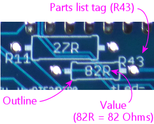
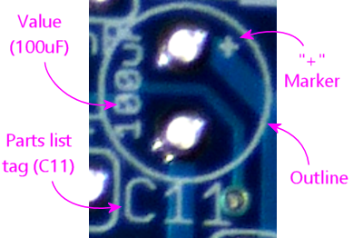
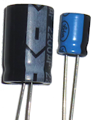
Component cheat-sheet
Matching the parts to their spots on the circuit board might seem a
little intimidating at first, but the "language" of the circuit board
markings is designed to make it as straightforward as possible. All
of the markings on the circuit board are there to let you see at a
glance what goes where. They also tell you how to orient the parts
where that matters. (Some parts, like resistors, don't care which
direction they go; other parts, like transistors and diodes, have to
be oriented the right way to work properly.)
There are only about a dozen different types of components on these
boards, so you'll see the same "footprints" used repeatedly. Once you
learn to recognize the common ones, you'll be able to quickly identify
the right parts.
Here's a quick visual reference to the circuit board markings for the
various component types. See the linked sections for more details on
the component type.
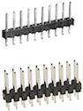
KL25Z sockets
The footprint on the circuit board for the KL25Z consists
of four slots that look like ordinary 0.1" pin headers:
Even though they look like the standard pin header footprints, they're
actually intended for 0.1" pin sockets, which look like this:
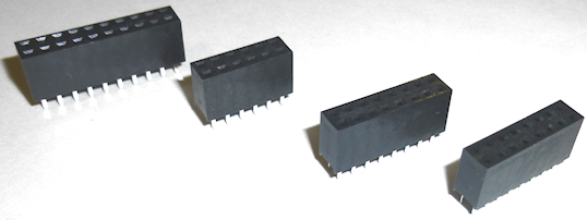
Those mate with the corresponding 0.1" pin headers, which you're
supposed to install on the bottom of the KL25Z (the side
without the IC chips).
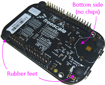
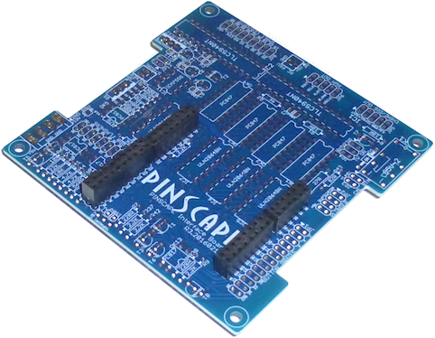
The KL25Z simply plugs into those sockets when you're done assembling
the board. Flip the KL25Z top-side-up so that the pins are facing
down, and plug the pins into the sockets on the main board.
But don't plug it in just yet! There are a bunch of parts on the
circuit board underneath where the KL25Z sits, so you'll need to leave
the KL25Z out for now while soldering parts there. For now, just
install the sockets on the main board, and the matching pin headers on
the KL25Z, and set the KL25Z aside. You can plug in the KL25Z when
the rest of the board is done. The KL25Z just plugs in, so it can
inserted and removed at any time; it's not permanently installed.
Special note on JP12 on the main board
This isn't mentioned anywhere in the parts list or on the board
itself, but you might want to omit the JP12 pin header on the
main board. Just leave that slot blank by not installing the
pin header.
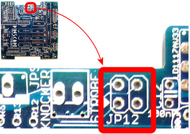
What this header is for: This header connects back to four unused GPIO
ports on the KL25Z. I call it the "expansion port", which I know is a
silly port name for an "expansion board", but it fits: this port is
for custom additions, if you want to make some custom mods to the
firmware to do something with those four free GPIO ports, and
similarly for future uses I might come up with some day that I haven't
thought of yet.
Why you might want to leave it blank: This header is really
confusingly marked (sorry I didn't notice this problem during the
design process). See how the word STROBE is written next to it, with
an arrow? A lot of people understandably take this to mean "Hey,
guys, the STROBE is over HERE!" But it doesn't mean that at all. The
STROBE marking is actually for the next pin header over, that little
2-pin header JP9. The arrow is just the "Pin 1" arrow used on most
of the headers, and isn't an "over here" kind of arrow at all.
The confusion is potentially harmful to the KL25Z, because it might
trick you into connecting the STROBE device to pin 1 on JP12. That
connects directly to a GPIO pin on the KL25Z, so connecting it to
a 12V strobe device can destroy the KL25Z.
Leaving out the pin header entirely will eliminate that risk.
Why you might want to install it anyway: There actually is one
thing that JP12 is good for with the current firmware: you can use it
for four extra button inputs. If you're going crazy with the buttons,
and you need more than the standard 24 button inputs already on the
main board, you can use JP12 to get an extra four.
You can always wait and install the header later if you decide you
need it. Or you can just install it up front now that you're aware of
which header is which. It's only a risk if you get confused about
which pin is for the STROBE, and hopefully that won't be a problem now
that you've read through all of this.
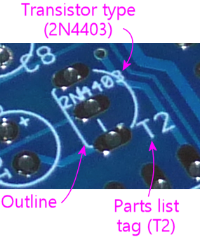
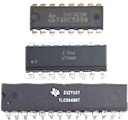
Special note on IC12 on main board
Note that the slot for IC12 (a 3.3V regulator IC chip) looks exactly
like the slot for a MOSFET (the big power transistors we use repeatedly
on the power board):
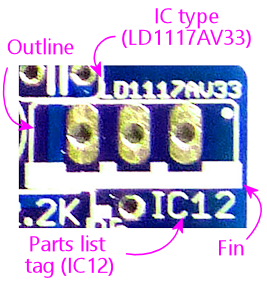
That's because this IC chip is packaged in a TO-220 case, which is
exactly the same case type used for all of our MOSFETs.
Installing this part is exactly like installing a MOSFET. The only
thing you have to be careful about is making sure you use the right
part! Don't install a MOSFET there; be sure to read the label on the
part and install the LD1117AV33 regulator chip. You can't tell the
difference just looking at the shape of the case - you have to read
the tiny text printed on the face of the case.
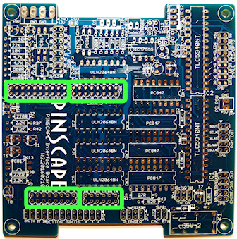
Special note on BYPASS resistors on the chime board
The chime board has eight resistors labeled BYPASS. Normally,
you don't install anything there. Just ignore this slot and
leave it empty. One less part to solder!
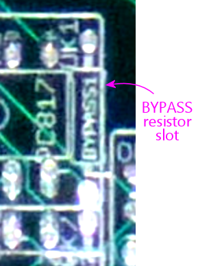
The BYPASS slot is there for the "Timer Bypass" option, which lets you
skip the timer protection circuits for the replay knocker and/or any
of the chime board outputs. See "Bypassing the timers on the chime
board" later in this section for details on how to do that.
Optional elements
Some of the components on the boards are optional. You only need to
install them if you want to use the features they implement.
Omitting the JP12 pin header on the main board
Read the "Special note about JP12" above for why you might want to
omit this pin header.
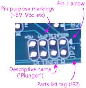
Configuring the "Small LED" current level
The "Small LED" ports on the main board (on pin header JP8) are
"constant current" outputs. This means that they have a built-in
current limiter that caps the current at a selected level, which
allows you to connect LEDs to these outputs directly, without
any current-limiting resistors. The function of the current-limiting
resistors is replaced by the built-in current limiter, eliminating the
need to install the resistors separately.
All of the Small LED ports have the same current limit, but you can
adjust what that common limit is, because it's determined by the value
of resistor R5. If you use the R5 value specified in the parts
list, 2.2K, the limit is set to 20mA. You can change this by using a
different value for R5.
You can select any value from 10mA to 60mA. To determine the resistor
value for a desired current level, use this formula:
(Resistance in Ohms) = 39060 ÷ (Desired current in milliamps)
For your convenience, here are some pre-figured values showing the
standard resistor sizes that approximate some selected current levels:
| Current | R5 value |
|---|---|
| 10mA | 3.9K |
| 20mA | 2K |
| 30mA | 1.3K |
| 40mA | 1K |
| 50mA | 750Ω |
| 60mA | 680Ω |
Don't use a resistor that would set a current above 60mA. Higher
currents might stress or even overheat the TLC5940 chip.
Any small-wattage resistor (1/8W or 1/4W) with the chosen Ohms value
will work here.
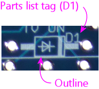
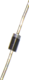
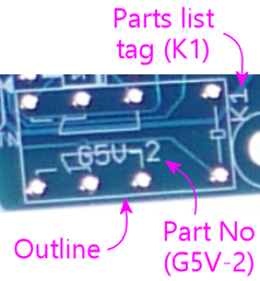
Omitting the TV relay
If you don't need the TV ON feature, you can simply omit all of the
following parts:
- D1 (1N4007)
- K1 (G5V-2 relay)
- OK15 (PC817)
- R39 (560R)
- R49 (2.2K)
- T6 (2N4401)
Omitting the TV IR remote features
If you don't need the IR remote control features, you can simply omit all
of the following parts:
- C2 (150nF)
- R7 (220R)
- R9 (2.2K)
- R11 (27R)
- T8 (2N4401)
- U$2 (TSOP38438)
Configuring the IR remote for 1 or 2 emitters
If you're including the IR remote control features, you can build it
to power either one or two IR "emitters" (the IR LEDs that transmit the
remote control signals).
Why might you want to use two emitters? To control two TVs! If you
use two emitters, you can place one near each TV's remote control
receiver, to ensure that both TVs get strong signals. Given the way
things are packed into a pin cab, it might not be possible to set up a
single emitter with a good line of sight to both TVs.
The only change you have to make between one IR emitter vs. two IR
emitters is the value for resistor R11 on the main board:
- For one IR emitter, use a 39Ω, 1/2W resistor for R11
- For two IR emitters, use a 27Ω 1/2W resistor for R11
When connecting two emitters, connect them in series. This
means that you wire then in a daisy chain:
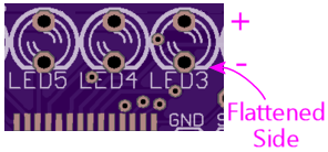
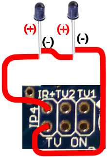 Recall that the longer leg of an LED is the positive (+) lead. IR
LEDs such as these emitters follow the same rule.
Recall that the longer leg of an LED is the positive (+) lead. IR
LEDs such as these emitters follow the same rule.
Omitting the knocker output
The whole knocker output circuit is optional. To remove it, simply
omit all of the following parts:
- C5 (1uF)
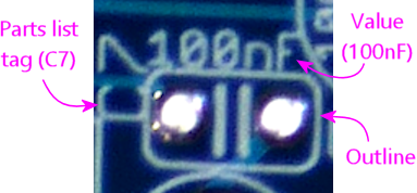
- C7 (100nF)
- C8 (1uF)
- C9 (100nF)
- IC11 (ICM7555)
- OK5 (PC817)
- Q1 (MOSFET)
- R6 (1M)
- R8 (2.2M)
- R10 (100K)
- R12 (100K)
- R12 (100K)
- R13 (47R)
- R14 (1K)
- R18 (47R)
- R37 (2.2K)
- T2 (2N4403)
- T3 (2N4401)
The list above includes all of the parts that make up both the
knocker's time-limiter circuit and the output control circuit, so if
you omit all of those parts, you can skip the section below about
bypassing the knocker output timer. The output timer won't be there
at all if you omit the parts above, so there's nothing left to bypass!
Bypassing the knocker output timer
The replay knocker output on the main board has a built-in hardware
timer that cuts off power to the output if it stays on continuously
for more than a couple of seconds. This is designed to protect your
replay knocker from software faults on the PC - it's been known to
happen that Visual Pinball can crash in the middle of an operation
that leaves the knocker coil energized. Leaving a knocker coil on for
more than a few seconds can overheat it and burn it up. However, if
you like to live dangerously, or if you want to re-purpose this output
for a different kind of device that doesn't need the timer protection,
it's possible to bypass the cut-off timer and turn this into a
general-purpose output with no time limiter.
Note: the procedure here omits just the timer part of the
circuit, leaving the output circuit for the knocker in place. If you
want to leave out the entire knocker circuit instead, including
both the timer and the output portion, see "Omitting the
knocker output" above.
To bypass the timer circuit and turn this into an un-timed, general-purpose
output:
- Omit all of the following parts (simply don't install anything
in their slots on the board):
- C5 (1uF)
- C7 (100nF)
- C8 (1uF)
- C9 (100nF)
- IC11 (ICM7555)
- R6 (1M)
- R8 (2.2M)
- R10 (100K)
- R12 (100K)
- T2 (2N4403)
- In place of the 47Ω resistor for R18, install an 82Ω resistor
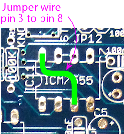
- Install a jumper wire between pins 3 and 8 of IC11 (remember, we're not
installing the IC there). "Jumper wire" just means that you can use an
ordinary piece of hookup wire.
With these changes, the replay knocker output will turn into an
ordinary, general-purpose, digital output with no timer cut-off.
"Digital" means that it's purely an on/off port: it doesn't have PWM
capabilities, so you can't use it for a device that requires
brightness or intensity control.
The power-handling capacity isn't affected by the timer bypass. No
changes are needed in the software (either in the Pinscape firmware
setup or on the PC), since it's invisible to the software in the first
place; the timer (when installed) acts to cut off power at the
hardware level without any software involvement.
The chime board's outputs are designed to be protected by hardware
timers, to prevent a coil from getting stuck "on" in case of a
software crash. If you wish, though, you can bypass the timers to
turn these outputs into ordinary, general-purpose outputs that you can
use for devices that don't need the timer protection. The timers can
be installed or bypasses individually for each output, so you create
any mix of timer-protected and general-purpose outputs on each board.
Bypassing a timer doesn't have any impact on the software on the KL25Z
or on the PC. The timers are completely invisible to the software,
since they intervene directly at the power switch level.
Note that the chimer board outputs are all "digital": they don't have
any PWM control capability, so you can't adjust the brightness or
intensity on one of these outputs. They can only be fully on or fully
off. That's true with or without the timer circuit.
To bypass an individual timer circuit:
- First, identify the timer block area for the output whose timer you
want to bypass. Each output has its own timer, and each timer can be
built or bypassed independently of the others. The timer block for a
each output is outlined on the board in a white rectangle. The blocks
correspond to the outputs as shown below - timer block 1 on the
diagram corresponds to output 1, etc.
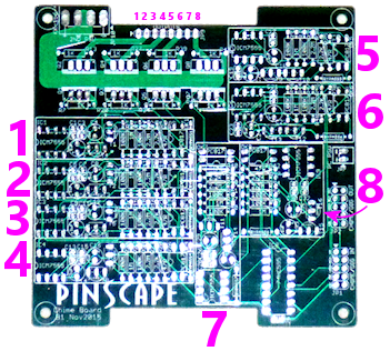
- You can also identify which block connects to which output by looking
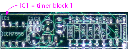
for the ICM7555 IC chip within the block. These are numbered the same
as the outputs: IC1 is in timer block 1 for output 1, IC2 is in timer
block 2 for output 2, etc.
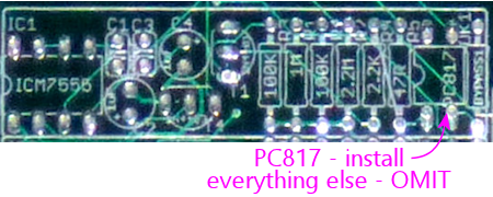
- Now we're going to build the "null" timer circuit, without the timer.
This means we're going to basically omit all of the normal parts.
- The only part from the original timer that you're going to install
here is the PC817 optocoupler chip, also labeled OKn
where n is the timer block and output number (OK1 for timer
block 1 and output 1).
- Now we're going to add two parts within this block that aren't
part of the normal timer circuit. First, find the BYPASS resistor slot.
It's the slot with a resistor footprint, labeled BYPASSn (n
is the block/timer number we're working with again).
- Install a jumper wire in that slot. In other words, simply
install a short piece of hookup wire between the two ends of the
resistor footprint.
- The second part is trickier. In the timer block, find the 2.2K
resistor and the 47R resistor that are placed right next to each other.
Every timer block has a pair like this. And there's a really unusual
marking on this pair: a white diagonal line across the pair.
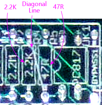
- That diagonal line is where you're going to install the second
extra part: a 220Ω resistor. Install it with one lead
going through the solder pad hole at one end of the diagonal line,
and the other lead in the solder pad hole at the other end of the
diagonal line. (As always for resistors, the orientation of the
resistor itself doesn't matter.)
And that's it! You've successfully converted this output into an
ordinary output with no timer cut-off.
- C5 (1uF)
- C7 (100nF)
- C8 (1uF)
- C9 (100nF)
- IC11 (ICM7555)
- R6 (1M)
- R8 (2.2M)
- R10 (100K)
- R12 (100K)
- T2 (2N4403)
