Appendix 1. KL25Z Pin Out
How to read the diagram
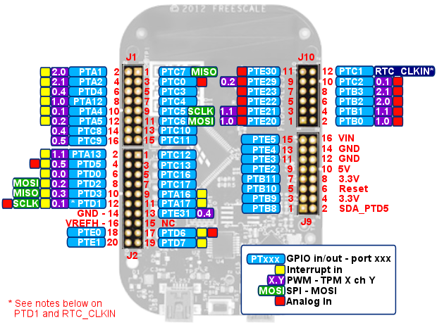
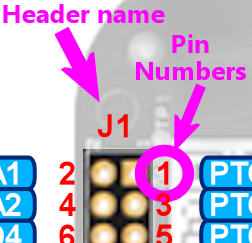 The diagram above shows all of the KL25Z's pin connections,
labeled by their "header" name and "pin number".
The diagram above shows all of the KL25Z's pin connections,
labeled by their "header" name and "pin number".
There are four headers - rectangular blocks of pins arranged in a
group. They're labeled J1, J2, J9, and J10.
In the diagram, each header's name is printed just above or below
header itself.
The pins on each header are numbered from 1 to however many pins are
on the header. The diagram shows each pin's number alongside the pin.
Throughout the Build Guide, we refer to individual pins using notation
like this:
J9-4
To find that pin, you go to header J9 and find pin 4
on that header.
The reason we use this notation is that the pin numbers by themselves
are ambiguous, since every header has a "pin 1" and a "pin 2" and so
on. You always have to know which header we're talking about to know
exactly which pin we're talking about. So we'll always tell you
something like "pin 7 on header J9", or the more compact shorthand
"J9-7".
Most (but not all) of the pins also have another name of the
form PTA1. The "PT" stands for "Port", and the "A1" is another
arbitrary label like the pin numbers. These range from PTA0 to PTE31.
You can see these names in the little blue boxes alongside the pins on
the diagram above. These are the names of the "GPIO" or "General
Purpose Input/Output" ports, which are electrical connections to the
KL25Z CPU itself. These are very important to us, because they're the
KL25Z's gateways to the outside world. They're where we can connect
buttons, sensors, and feedback devices.
The other markings on the diagram alongside the GPIO port names
indicate the "capabilities" of each port. The KL25Z's physical wiring
gives special capabilities to certain ports. The capabilities are
important to understand if you're writing software for the device
or working it into a hardware design, but you won't have to worry
about these if you're using the Pinscape software, since it
already takes all of this into account. The Pinscape Config Tool
will guide you to the proper port selections whenever special
capabilities come into play.
PTD1 and the blue on-board LED
The port labeled PTD1 needs some additional explanation. It's a GPIO
port, but it's also hard-wired on the KL25Z to the blue segment of the
KL25Z's on-board status LED - the RGB LED that normally shows the
Pinscape firmware's current status by flashing various color patterns
(KL25Z Status Lights).
You can use PTD1 as a feedback device output port if you wish, simply
by assigning it to an output port row in the Pinscape Config Tool. If
you do, its output port use automatically supersedes the status light
usage in the Pinscape firmware, so there won't be any conflict at the
software level. However, be aware that the on-board wiring to the
blue LED will still be there. The blue LED wiring is a fixed,
physical feature of the KL25Z board that can't be changed in software.
This means that the blue LED segment will turn ON whenever the PTD1
pin is at a "low" voltage, and OFF whenever PTD1 is "high". So the
blue LED will light up when the feedback port is OFF and turn off when
the feedback port is ON. You can just ignore that if it doesn't
bother you, or you can modify the KL25Z as described below to sever
the on-board wiring to the LED.
You can also use PTD1 as a button input port, again, simply by
assigning it in the Config Tool. As with using PTD1 as an output
port, using it as a button input port will automatically supersede its
use to control the Pinscape status LED indicator, so the blue segment
of the status light will stop functioning. And as with using PTD1 as
an output port, using it as an input port won't actually remove the
physical connection between the PTD1 pin and the blue LED. The effect
as an input port will be that the blue LED will turn on whenever you
press the connected button. That should be harmless, but if it
bothers you, you can use the procedure below to sever the internal
wiring to the blue LED.
I wouldn't attempt to use PTD1 for any other purpose (such as a
plunger input, TLC5940 output, etc) unless you sever the LED
wiring as described below. The LED wiring shouldn't interfere with
using PTD1 as a feedback output port or button input port, but it
could create problems for other uses, since it places an electrical
load on the pin in addition to whatever else you're connecting. That
could definitely interfere with using the port as an analog input or
for any high-speed signal I/O.
Severing the on-board wiring between PTD1 and the blue LED: To
break the connection to the on-board LED and turn PTD1 into a true
general-purpose port, remove resistor R11 on the
KL25Z board. R11 is a small surface-mount resistor on the top of the
board; see the diagram below to help find it. It's labeled with the
text "R11" next to the part, so double-check the printed label to make
sure you've identified the right part.
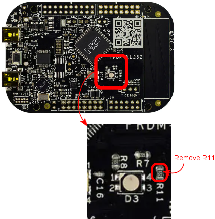
R11 isn't too hard to remove, since it has a fair amount of empty
space around it on the board. My approach to removing it would be to
use a pair of forceps to take hold of the part, and then touch a
soldering iron to the part to melt the solder, pulling away gently
with the forceps until the part pulls free. You could also just use
the tip of the soldering iron to apply some gentle sideways pressure
to the part while heating it. Continue pressing it until it comes
loose, then flick it away so that it doesn't reattach as the solder
cools.
If you do sever the blue LED wiring, the blue component of the
Pinscape status indicator light will obviously stop working. That
will disable all of blue elements of the flash patterns, and will
change purple elements to red.
RTC_CLKIN (PTC1, J10 pin 12)
Port PTC1 has a special assignable usage, as the reference clock
signal input for the real-time counter, which the KL25Z documentation
refers to as RTC_CLKIN. This provides an external reference clock
signal (a square wave running at a specific frequency) for the KL25Z's
on-board real-time module. The RTC is designed to perform
time-keeping functions, particularly related to scheduled events.
The Pinscape software doesn't currently use the RTC module, so this
pin is free for use as an ordinary GPIO pin.
If any features are ever added to the Pinscape software that require
the RTC module to be activated, this pin will have to be used for the
clock input whenever those features are activated. I don't
contemplate any such features currently, and even if some future use
does become interesting, it would be optional - you'd only have to
reassign PTC1 to that usage if you enabled the new feature.
(The pin is actually hard-wired on the KL25Z to a pin on the separate
SDA CPU - the one that runs the boot loader, for installing new
firmware versions. This is designed so that the SDA CPU can be
programmed to generate the required external clock signal for the RTC
module. The mbed version of the boot loader unconditionally generates
that signal on this hard-wired connection, so if the mbed boot loader
is installed, PTC1 can't be used as a GPIO pin - the clock generator
feeds a 32768 Hz square wave into this pin, making it effectively
impossible to use for anything else. Fortunately, the standard
PCMicro boot loader that comes with the KL25Z doesn't do this; it
leaves the connected SDA CPU output port in a high-Z state, which
effectively turns the hard-wired connection into an open circuit and
thus allows us to use the GPIO pin normally.)
SDA_PTD5 (J8 pin 2)
This is another unusual pin that can't be used for any Pinscape
function.
Even though the name makes it sound like a GPIO pin, this pin doesn't
connect into the KL25Z CPU at all. Instead, it connects to a separate
chip on the board where the boot loader resides. "SDA" is Freescale's
name for their boot loader system, which is why this pin is labeled
SDA_PTD5 instead of just plain PTD5. Confusingly, the boot loader
chip has its own set of GPIO ports, with basically the same naming
convention as the KL25Z's ports. That's why the name looks like a
GPIO pin - it is a GPIO pin, just not a KL25Z GPIO pin. That
means that it's not usable for Pinscape purposes, since the Pinscape
software has no way to access the pin.
USB Ports
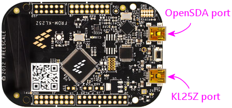
(Note that the ports are labeled in fine print on the bottom
side of the KL25Z, so you don't have to just remember which is which.)
The "KL25Z port" is the one that's connected to the microcontroller
proper. This is the port that the Pinscape software uses for its USB
joystick, keyboard, and LedWiz emulation interfaces.
The "OpenSDA" port isn't connected to the microcontroller.
It's connected to a separate processor on the board that's there for
the sole purpose of downloading firmware into the microcontroller's
flash memory. That separate processor isn't involved in any of the
Pinscape functions, so the OpenSDA port doesn't need to be connected
at any time except when installing new firmware. But it's also
harmless to leave it plugged in all the time - leaving it plugged in
doesn't interfere with normal Pinscape operations. The OpenSDA
processor just sits there emulating a thumb drive awaiting firmware
downloads.
About the KL25Z
The KL25Z is a single-board computer, incorporating a 32-bit
ARM-architecture CPU (Cortex M0+), 16K SRAM, numerous on-board
peripheral devices within the CPU (three PWM modules, a 4-channel DMA
controller, real-time clock, SPI and I2C bus interfaces, a USB 2.0
host/device controller, three UARTs, an analog-to-digital converter, a
digital-to-analog converter, a flash memory controller, and more), and
additional peripherals on the board but external to the CPU (a
three-axis accelerometer, a touch sensor, a clock generator, and an
RGB LED).
The board also includes an integrated "programmer" module with its own
separate USB connection. This is what allows us to download new
firmware, such as the Pinscape Controller software, directly from a
Windows machine.
GPIO ports and special functions
All told, the KL25Z CPU chip (not the board, but the chip itself)
exposes about 80 external connections. About 50 of these connections
are exposed through header pins on the KL25Z board. The rest are
mostly dedicated to connections with the on-board peripherals; these
aren't exposed externally as they can't be reassigned. That's part of
why you find the gaps in port numbering on the exposed pins.
Most of the external header pins on the KL25Z are wired to GPIO ports
("general-purpose I/O"), which can be connected to external
electronics to send digital signals to and from the KL25Z CPU. The
diagram above shows the layout of the header pins and the GPIO port
assignments. The pin layout can't be changed by the software; the
pins are physically wired this way on the board.
In addition to the basic GPIO functions, many of the pins can also be
connected, under software control, to one or more of the on-board
peripherals. As with the GPIO port assignments, the set of these
possible connections for each pin is hardwired: each pin can only
perform certain special functions. The diagram shows which special
functions are available on each pin. The software determines which
special function a given pin performs at any given time using another
on-board peripheral called the "multiplexer". This is a essentially a
switchboard that connects pins to special modules. At any given time,
a pin can only be connected to one module. For example, a pin that's
PWM-capable only generates PWM signals when the software tells the
multiplexer to connect the pin to the PWM module.
PWM limitations
The KL25Z hardware has some rather complex limitations on its PWM
outputs. The diagram tries to make these evident, but you have to
understand the nature of the limitations to make sense of the
information in the map.
The KL25Z generates PWM signals (pulse-width modulation) through
on-board peripherals called TPMs (Timer/PWM Modules: yes, it's a
nested acryonym). The CPU has three of these modules: TPM0, which has
6 channels; TPM1, with two channels; and TPM2, with another two
channels. That's ten channels total across the three modules.
If you look at the diagram, you'll see that there are 23 GPIO pins
marked as PWM-capable. This brings us to the first limitation. You
can't actually have 23 separate PWM outputs, despite the 23
PWM-capable pins. The PWM signal reaching the pins has to be
generated in the TPM module channels, and as we've seen, there are
only 10 of these channels in all. Take a look at the map and find
PTA1 and PTB2. You'll see these are both marked "2.0" in their PWM
boxes. That means both of these pins are assigned to TPM2 channel 0.
You can assign both of these channels as PWM outputs, but if
you do, you won't be able to control them independently, because they
both get their signals from TPM2.0. Change the brightness on one pin
and you'll change it to the same setting on the other pin. So despite
the 23 PWM-capable pins, you can really only use 10 of them as PWM
outputs at once.
The subtler limitation is in the pulse frequency generation. The
duty cycle of a PWM output is controlled by its channel.
However, the period of a PWM output is controlled by its
module. All of the channels on a given module share the same
period (or, equivalently, frequency). Many PWM applications don't
care very much about the frequency, but the frequency is critical for
some purposes. For example, if we're using the PWM signal as a clock
generator for an external device, we need an exact frequency setting.
This means that if we need two such clocks at different frequencies,
we have to assign the two functions to pins that map to separate TPMs,
to given them independent control over the frequency.
The ability to set independent frequencies isn't just academic. It
actually matters for Pinscape if you're using the expansion boards
and/or the IR functions:
- The expansion boards use a PWM output to generate the master clock signal for the TLC5940 chips (called the "grayscale clock" in the TLC5940 data sheet). This master clock frequency isn't set in stone, but it's constrained by a number of factors: it has to be fast enough that the strobing effect isn't visible to the eye, and its upper limit is constrained by the KL25Z's data transmission speed, the ability of the physical wiring to conduct signals reliably, and the TLC5940 chip's design limits. For the full technical details, refer the TLC5940 driver source code in the Pinscape firmware (TLC5940/TLC5940.h in the source tree). The setting as of this writing is 350 kHz.
- The IR transmitter uses a PWM channel to generate the IR carrier frequency. This frequency is determined by the IR protocol being used for a given transmission, so it can vary from one transmission to the next. The protocols currently implemented use carrier frequencies ranging from 36kHz to 40kHz.
The requirements for these features to use specific PWM frequencies,
combined with the limitations of the KL25Z's TPM hardware, has two
important practical implications:
- First, the TLC5940 interface's master clock port and the IR
transmitter's data output port must be assigned to GPIO ports
that use separate TPM units. Each function requires the
ability to set its own frequency independently of other PWM usages,
and since the frequency of a PWM output is set at the TPM unit
level, each function must have free control over an entire TPM unit.
Therefore each must be assigned to a separate TPM unit.
The Pinscape Config Tool knows about this requirement, and it will automatically guide you to select appropriate GPIO pins if you're using both functions. It'll warn you if you attempt to assign the two functions to the same TPM unit. You must not ignore these warnings; the device won't function properly if you do.
- Second, if you're using a TLC5940 chip and/or the IR transmitter,
and you're also using GPIO ports as regular feedback output
ports, be aware that the GPIO ports you're using might have their PWM
frequencies fixed by the TLC5940 or IR transmitter functions. This
might be an issue if you're using booster circuitry with the outputs,
because the TLC5940 clock setting is a high frequency that might be
too fast for booster circuits. Booster circuits that use optocouplers
in particular might not work properly, because most optocouplers have
a speed limit of about 80kHz, well below the TLC5940's 350kHz setting.
You can mitigate this by assigning your PWM feedback outputs to GPIO ports that use other TPM units. Refer to the matrix below for the associations between GPIO pins and TPM units.
Here's a matrix showing the available GPIO ports for each TPM unit.
Remember, the frequency of a PWM port is set at the unit
level, so all of the ports associated with TPM Unit 0 will operate
at the same frequency, all of the ports assigned with Unit 1 will
operate a second common frequency, and all of the ports on Unit 2
operate on a third common frequency. Each channel represents
a separately controllable duty cycle that operates at the
common frequency for its unit. For example, PTA4 and PTC2
are both on Unit 0, Channel 1, so they represent the same PWM output;
they can't be separately controlled, as they share the same frequency
(set on Unit 0) and the same duty cycle (set on Unit 0 Channel 1).
| TPM Unit | Channel | GPIO ports |
|---|---|---|
| 0 | 0 | PTD0 |
| 1 | PTA4, PTC2, PTD1 (blue on-board LED) | |
| 2 | PTA5, PTC3, PTD2, PTE29 | |
| 3 | PTC4, PTD3, PTE30 | |
| 4 | PTC8, PTD4, PTE31 | |
| 5 | PTC9, PTD5 | |
| 1 | 0 | PTA12, PTB0, PTE20 |
| 1 | PTA13, PTB1, PTE21 | |
| 2 | 0 | PTA1, PTB2, PTB18 (red on-board LED), PTE22 |
| 1 | PTA2, PTB3, PTB19 (green on-board LED), PTE23 |
Why is the pin layout so random?
Blame the Arduino.
The layout is as it is because the KL25Z's designers took Arduino
compatibility as the starting point. The Arduino is a popular
hobbyist platform that started off on some rather primitive 8-bit
hardware. One of the features was a very rigid assignment of
particular functions to particular pins - PWM output, analog in, UART
RX/TX, etc. The KL25Z is much more flexible in the way it maps these
special functions to pins, but it's not infinitely flexible; it too
can only expose certain functions on certain pins. In order to
achieve the desired pin compatibility with the Arduino, the KL25Z's
designers had to arrange the pins in the peculiar order we find them
in here. This arrangement allows the pin at each physical position to
be assigned to its traditional Arduino role, which allows some Arduino
add-on boards to be used directly with a KL25Z. (But be careful if
you plan to do this, because there is one other major difference
between the Arduino and KL25Z that can seriously affect compatibility:
voltage. Most Arduinos run on 5V, whereas the KL25Z is a 3.3V device.
The KL25Z will be damaged if exposed to 5V levels on any of its GPIO
pins. Many Arduino add-ons generate 5V signals, which makes them
incompatible with a KL25Z even if the pin layout matches.)
