PWMWorker is a firmware program for the Raspberry Pi Pico that turns the Pico into a PWM (Pulse-Width Modulation) controller chip, in imitation of dedicated PWM chips like TLC59116 and PCA9685. Like those chips, PWMWorker provides an I2C interface that lets a host microcontroller (for example, another Pico, perhaps running the Pinscape Pico firmware), control a set of output pins with PWM.
The mainstream chips in this class are designed primarily to control arrays of LEDs (indeed, the category where you'll find most of them listed on Mouser and DigiKey is "LED driver chips"), but there's really nothing that limits them to LEDs, since the output ports are ultimately just electronic switches. They can be used to switch almost any sort of device, especially if the output ports are used as inputs to amplifier circuits that increase their current and voltage drive limits. In virtual pinball machines, they can be used to control feedback devices, including lights, solenoids, and motors. And even though the chips are nominally PWM controllers, the PWM capability doesn't have to be exercised for every port; a port can equally well act as a simple on/off switch for a device that doesn't need (or can't use) PWM, simply by limiting the duty cycle settings on that port to 0% and 100%.
PWMWorker was created as part of the Pinscape Pico project, but it's a completely standalone device that can be used in any project that calls for a PWM controller chip. Any host microcontroller compatible with a 3.3V I2C bus can be used, and you don't need any Pinscape software on the host controller, since PWMWorker provides a well-defined and fully documented I2C register interface.
This data sheet documents the Pico PWMWorker system from the perspective of a hardware designer who wishes to use the device as part of a circuit board, in place of one of the more conventional PWM controller chips. It describes how to wire the Pico into your circuit board at the hardware level, and how to access the I2C interface to control the device from your main I/O controller's software. PWMWorker's I2C command set is very similar (intentionally) to the interfaces exposed by most of the commercial PWM controller chips (which are mostly very similar to one another), with the goal of making it relatively easy to adapt a host-side software driver that you've already created for one of those other chips to this new "chip". This design doesn't attempt to be a drop-in replacement for any specific commercial chip, but it's meant to be similar enough to those chips in its conventions that it's a low-effort substitute.
The PWM outputs are implemented as Pico GPIOs, so each output port is a 3.3V push-pull driver capable of sourcing and sinking about 10mA per pin. This makes the device suitable for driving small LEDs directly. Ports can also be used to drive larger loads by connecting them to amplifier circuits that accept logic-level inputs; several examples of suitable booster circuits are presented later in this document. Ports can be configured with active-high or active-low outputs, providing the flexibility to use amplifier circuits that require either kind of trigger level. The ports can be enabled and disabled as a group.
At Pico reset, all GPIO ports (and thus all of the OUTn ports) are configured as inputs, which connects the ports to GND through a high-value resistor (about 50K ohms) internal to the Pico. This is the OUTn port state we refer to as "disabled". This makes it possible to design external booster circuits for glitch-free startup - that is, guaranteeing that all amplified output ports remain OFF throughout the power-up and software initialization process, without even brief activation.
Features, benefits, and tradeoffs:
| Pin Name | Description |
|---|---|
| OUT0 | Output port #0 (GP0 on the standard Pico pin-out diagram) |
| OUT1 | Output port #1 (GP1 on the standard Pico pin-out diagram) |
| OUT2 | Output port #2 (GP2 on the standard Pico pin-out diagram) |
| OUT3 | Output port #3 (GP3 on the standard Pico pin-out diagram) |
| OUT4 | Output port #4 (GP4 on the standard Pico pin-out diagram) |
| OUT5 | Output port #5 (GP5 on the standard Pico pin-out diagram) |
| OUT6 | Output port #6 (GP6 on the standard Pico pin-out diagram) |
| OUT7 | Output port #7 (GP7 on the standard Pico pin-out diagram) |
| OUT8 | Output port #8 (GP8 on the standard Pico pin-out diagram) |
| OUT9 | Output port #9 (GP9 on the standard Pico pin-out diagram) |
| OUT10 | Output port #10 (GP10 on the standard Pico pin-out diagram) |
| OUT11 | Output port #11 (GP11 on the standard Pico pin-out diagram) |
| OUT12 | Output port #12 (GP12 on the standard Pico pin-out diagram) |
| OUT13 | Output port #13 (GP13 on the standard Pico pin-out diagram) |
| OUT14 | Output port #14 (GP14 on the standard Pico pin-out diagram) |
| OUT15 | Output port #15 (GP15 on the standard Pico pin-out diagram) |
| OUT16 | Output port #16 (GP16 on the standard Pico pin-out diagram) |
| OUT17 | Output port #17 (GP17 on the standard Pico pin-out diagram) |
| OUT18 | Output port #18 (GP18 on the standard Pico pin-out diagram) |
| OUT19 | Output port #19 (GP19 on the standard Pico pin-out diagram) |
| OUT20 | Output port #20 (GP20 on the standard Pico pin-out diagram) |
| OUT21 | Output port #21 (GP21 on the standard Pico pin-out diagram) |
| OUT22 | Output port #22 (GP22 on the standard Pico pin-out diagram) |
| OUT23 | Output port #23 (GP28 on the standard Pico pin-out diagram) |
| SDA | I2C bus data (SDA) connection |
| SCL | I2C bus clock (SCL) connection |
| GND | Connected internally on the Pico to its power supply and USB ground |
| VBUS | USB bus power (output); connects the USB port's +5V |
| VSYS | Pico power chain input port |
| 3V3 (OUT) | Output from the Pico's internal 3.3V regulator |
| 3V3_ENABLE | Enable control for the Pico's internal 3.3V regulator |
| ADC_VREF | Voltage reference for the Pico's on-board ADC |
| RUN | Pico RUN/RESET control port; pulling to GND reset the Pico |
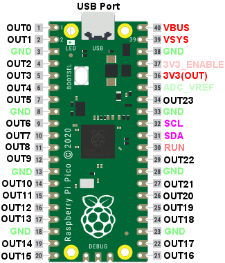
OUT0 through OUT23 are the PWM output ports. These are standard Pico GPIO ports, although note that we use our own labels - these aren't the native GPn lables. Our OUTn port numbering almost matches the Pico's native GPn port numbering, the one exception being GP28, which we label OUT23.
(It seemed more important to number the ports consecutively in the I2C software model than to strictly match the GPn numbering, because (a) this makes the software model more sensible if you approach it strictly at the I2C interface level, and (b) it makes the correspondence between OUTn port numbers and I2C register addresses easy to express arithmetically. Host device driver software would be unnecessarily complicated if it had to work in terms of a discontiguous port numbering scheme. On the other hand, we didn't make the numbering arbitrarily different where it didn't have to be. The only reason that we didn't maintain a perfect correspondence is that the Pico doesn't have an exposed GP23, so there was simply no way to make OUT23 match its GP number no matter which GP we mapped it to.)
The I2C interface allows the host to enable or disable all outputs as a group; at reset, all outputs are disabled, allowing the host to configure outputs before they start driving their connected loads. When outputs are disabled, all of the OUTn pins are configured in INPUT mode, which connects them to GND through a high-value internal resistor in the Pico (about 50K). When ports are enabled, the GPIOs are reconfigured in OUTPUT mode, which makes them push/pull drivers at 3.3V. Each port in OUTPUT mode is capable of sinking or sourcing up to about 10 mA, which makes them suitable for driving small LEDs directly. For larger loads, an amplifier circuit with a logic-level trigger input must be used. The host can configure ports individually to use active high or active low logic, which provides the flexibility to use amplifiers that trigger on either high or low input levels.
GND ports connect to the Pico DC ground, which is also the USB ground (if plugged into USB). These ports should be connected to your carrier board's DC ground.
SDA and SCL are the I2C ports. Connect these to the corresponding ports on your I2C "master" device (typically the main I/O controller in your design, such as a Pinscape Pico). The Pico is a 3.3V device, so the bus must run at 3.3V logic. As always with I2C bus designs, both bus lines must be (separately) pulled up to 3.3V with suitably sized resistors. The exact resistor size required depends upon the overall bus capacitance and the SCL clock speed (400 kHz for this device); on-line calculators are available for figuring the required sizes, but most I2C devices are tolerant enough about timing that you can often get away with choosing something in the 2K to 4K range more or less arbitrarily.
VBUS, VSYS, and 3V3(OUT) are hooks into the Pico's power chain, which is well documented in the Rasbperry Pi Pico Data Sheet; refer to the section titled Powering Pico. The VSYS port can be used to power the Pico as an embedded component, without the need for a USB connection, as long as certain precautions are observed. In particular, the VSYS input must be protected against reverse flow into the power supply when the USB cable is connected. See the Pico data sheet for details. If the Pico is to be plugged into USB at all times, that will supply the Pico with power, so no separate VSYS power input is needed.
3V3_OUT is the output from the Pico's internal 3.3V regulator. This can be used to power other peripherals with 3.3V power. This will typically be left unconnected in a PWMWorker application.
3V3_ENABLE and ADC_VREF should be left unconnected for a PWMWorker application.
No USB connection is required for normal PWMWorker operation. The only time a USB connection is needed is when you're installing or updating the PWMWorker firmware. The Pico communicates with its host I/O controller purely through the I2C bus interface during normal operation, and doesn't use the USB port.
However, there's also no harm in maintaining a continuous USB connection during normal operation. In fact, this is one way that you can provide power to the Pico.
The diagram below shows a typical application circuit, with the PWMController Pico connected to a host microcontroller. Any type of microcontroller can be used as the host, as long as it's compatible with a 3.3V I2C bus. Microcontrollers with higher or lower logic voltages may also be used, by placing voltage level shifters on the SDA and SCL lines between the Pico and the main bus.
The PWMWorker Pico does not need a USB data connection, since it communicates solely via the I2C bus connection. However, a USB connection can be used as the power source if desired.
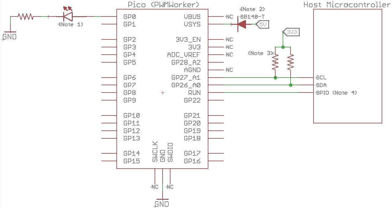
The output wiring is shown for a simple LED with high-side control, but this can be replaced with any circuit that can be driven by a Pico GPIO output. Pico outputs can drive up to about 10mA at 3.3V directly, and can drive almost any type of load with a suitable amplifier/booster circuit. Several example circuits that can drive higher-current devices are shown in the section below. Each output driver is independent, so you can freely mix and match driver types across the various outputs.
The Pico can be powered through its USB port, or through the Pico's VSYS power chain input. Various methods for powering the Pico through the VSYS pin are described in the Rasbperry Pi Pico Data Sheet; refer to the section entitled Powering Pico.
If you do choose to power the Pico through VSYS, please pay close attention to the advice in the Pico Data Sheet about protecting against power flowing back into the VSYS supply when USB is also powered. This is most easily accomplished by placing a Shottky diode between the 5V supply and the VSYS input, as shown in the sample application circuit above.
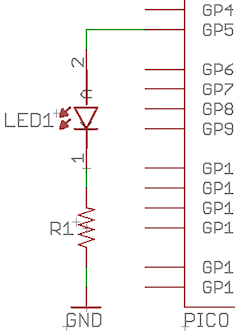
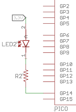
Small LEDs can driven directly from the Pico's GPIO ports at up to about 10mA of forward current. GPIO ports in OUTPUT mode act as push/pull drivers at 3.3V, so you can use a Pico port as either a high-side or low-side switch. Since Pico ports will only tolerate 3.3V, they can only directly drive LEDs with forward voltages less than 3.3V. Most red LEDs have forward voltages of 2V or less, but some other colors require 3.4V or higher. LEDs with higher forward voltages will require an amplifier circuit, discussed in the next section.
The Pico's output ports don't provide any current limitation, so you must provide a current-limiting resistor for each LED.
High-side switching: The simplest way to connect an LED is to use the GPIO port as a high-side switch, where the Pico provides the positive supply voltage to the LED's anode, and the LED's cathode is connected to GND.
Low-side switching: The GPIO port can also be used as a pseudo low-side switch, where the Pico provides the ground connection, and the LED's anode is connected to 3.3V power. This configuration is necessary if you're driving a device with multiple channels (e.g., an RGB LED) where the anodes are all wired together, known as the "common-anode" configuration. Since the anodes can't be switched individually, you have to do the switching on the cathode (GND) side.
Low-side switching requires the port to be configured as Active Low using the CONFn port configuration register (see the I2C register list below). In Active Low mode, the port will be driven to 3.3V during the OFF portion of the PWM duty cycle, and 0V during the ON portion. During the OFF portion, then, both ends of the LED are at 3.3V, so there's no voltage potential across the LED, and it turns OFF. During the ON portion of the duty cycle, the port drops to 0V, creating a positive voltage across the LED that allows it to turn ON.
Note that this is only a "pseudo" low-side switch. A true low-side switch would be in high-impedance state during the OFF portion of the duty cycle. In this case, the port is at the 3.3V supply voltage during the OFF portion. When used with a 3.3V device, this acts like a low-side switch, by preventing current from flowing during the OFF phase and allowing it during the ON phase. However, a true low-side switch would be usable with devices with different supply voltages, which this is not; this can only be used with a 3.3V device. Using a device with a supply voltage higher than 3.3V would expose the GPIO port to the higher voltage, which might destroy the Pico, as its ports can only tolerate 3.3V inputs.
An amplifier or "booster" circuit of some kind is required if you wish to use the Pico to drive a load of more than around 10mA or with a supply voltage other than 3.3V.
Since a PWMWorker Pico is physically just an ordinary Pico, any amplifier circuit designed to work with a Pico generically will work. The Pico is a popular device with a great deal of information on it published on the Web, so you should be able to find many examples of circuit designs that will work with it with a little Googling. But to save you some legwork, the sections below provide a few simple but flexible building-block circuits that can be used in many applications.
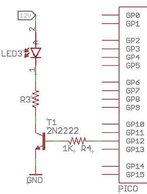
The simplest type of booster circuit is an NPN transistor switch. Small-signal transistors like 2N2222 can switch loads up to a few hundred milliamps and 30V to 50V. An NPN works best as a low-side switch, where it connects to the GND end of the load being driven. Note that even though the NPN is acting as a low-side switch, the control input to the switch - which is what the GPIO output port provides - is still Active High: the LED turns ON when the GPIO port output is HIGH. So you'd configure the port in the default Active High mode for this design.
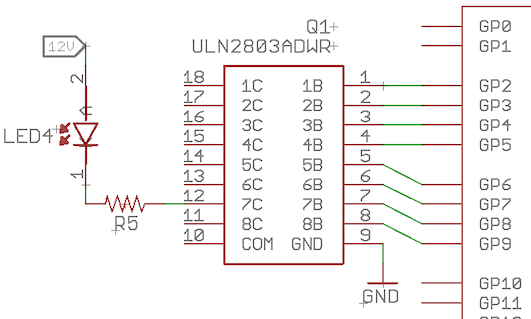
Darlington transistors can control higher currents than small NPN transistors, and there are several chips available that implement multiple channels (typically 8) of Darlington outputs in a single package, such as ULN2803A. ULN2803A is particular convenient for microcontroller applications like this one, because the chip includes internal current-limiting resistors for the input ports, so that the GPIO ports can be directly connected to the Darlington input ports. This reduces the part count, saving money and assembly work.
For really high-power devices, like solenoids and motors, you need a MOSFET, specifically a large "power" MOSFET. Many power MOSFETs are available that can switch 10A and up, at 50V or more, which makes the MOSFET the device of choice for controlling anything larger than an LED from a microcontroller. But MOSFETs are somewhat more challenging to control than NPNs and Darlingtons, because most power MOSFETs are all by themselves high-power devices that are above the limits of a Pico GPIO port to control directly. In particular, most power MOSFETs require voltages well above 3.3V for their control input signal, and many also require higher current than a Pico GPIO port can provide, especially when operating at high PWM frequencies. So you need an amplifier to drive your amplifier! There are numerous ways to do this, but the easiest and best is to use one of the many special "gate driver" chips that are purpose-built for this application. One good example is UCC27524P. A circuit based on this chip is shown below. Using a gate driver like this makes the circuit much more forgiving about the MOSFET specs it requires, giving you more flexibility when choosing parts. The circuit here will work with most power MOSFETs, as long as they're safe to use with the 12V gate drive shown (check the VGS limit in the Absolute Maximum Ratings in the data sheet; most large power MOSFETs have a rating around 20V).
A gate driver chip is particularly beneficial for the Pico because of the high PWM frequencies the Pico is capable of. MOSFETs produce the most heat when they're in their "switching" phase, between fully OFF and fully ON. The time it takes to complete this transition isn't affected by the switching frequency, so when you increase the PWM frequency, you increase the percentage of time the device spends in the heat-producing switching zone, which makes the MOSFET get hotter faster. One way to mitigate this is to reduce the PWM frequency; another is to make the switching time faster. The switching time is a function of the MOSFET's physical properties, and of the gate driver, so one way to make it faster is to make the gate driver faster. That's what gate driver chips like UCC27524P are all about: they're designed specifically to make the MOSFET turn on and off as quickly as possible, by delivering rapid bursts of current at each switching transition. That allows you to operate the MOSFET at higher frequencies with less heating.
Note that this circuit is designed for use with N-channel enhancement-mode MOSFETs only. The other common type, P-channel, is essentially a polarity-reversed version that won't work in this circuit.
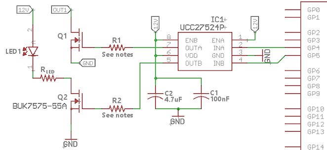
Selecting gate resistors R1, R2: 220 Ohms seems to be a good general-purpose choice. The primary purpose of these resistors is to suppress "ringing", which refers to high-frequency current oscillations that occur during the rapid inrush of charge when the MOSFET gate is initially switched on. For that function, you only need a very small resistor, on the order of 10 Ohms. However, the resistors have a second function, which is to protect the UCC27524P chip from excessive current spikes during on/off switching. UCC27524P's entire purpose is to handle high-current spikes, but even so, it has its limits. The chip has to dissipate a certain amount of heat during on/off switching transitions, and since PWM operation is all about rapid on/off switching, high PWM frequencies increase the amount of heat the chip has to dissipate. R1 and R2 limit the current spikes during switching transitions, which in turn reduces the power dissipated by the chip. Higher R1 and R2 values lead to less chip heating, but the trade-off is more MOSFET heating, because they slow down the MOSFET switching time and thus cause more switching power losses. So we have one of those cruel trade-offs: you can either heat up the driver chip, or you can heat up the MOSFET, take your pick. The optimal R1 and R2 values have to balance that tension between faster MOSFET switching (lower R1/R2 values) and safer driver chip operation (higher R1/R2 values). The 220 Ohm recommendation that opened this note was chosen as a one-size-fits-all compromise. It's high enough, experimentally, to protect UCC27524P from damage when using a MOSFET with a high gate charge rating (IRF540N), but it's low enough to handle fast PWM rates (20 kHz) without excessive MOSFET heating due to switching power loss. Note that higher gate charges are more difficult for this circuit to handle, so you'll make it easier on the circuit if you pick a MOSFET with a lower gate charge. (You can find the gate charge listed in the data sheet, usually under the parameter named Qg.) But MOSFETs with lower gate charge values tend to be more expensive, so the circuit is designed to accommodate a range of devices, to give you some flexibility to be cost-conscious when selecting parts.
See this vpforums thread for some more discussion on the resistor selection: www.vpforums.org/index.php?showtopic=54968&p=543950.
When output ports control mechanical devices, it's desirable to design the output circuits for "glitch-free startup", meaning that the devices are deterministically OFF throughout the initial power-up period. There's necessarily a short time interval between when power is first applied to the device, and when the software has finished initialization and is in control of the output ports. During this time, the software isn't able to control the electronic state of the output ports (since the software isn't fully running yet), so it's up to the hardware design to ensure that devices remain OFF during this time.
The Raspberry Pi Pico has internal circuitry that provides a deterministic electronic state on the ports during the initial power-on reset period. The Pico sets all GPIO ports to INPUT mode at reset; in this state, each GPIO is connected to GND through a high-value (50K ohm) resistor internal to the Pico. Ports remain in this state until the firmware program explicitly reconfigures them.
PWMWorker extends this period of deterministic INPUT port state throughout its own initialization, and through the completion of the host controller's initialization (the host controller is the I2C bus master that's sending commands to the PWMWorker). PWMWorker holds all ports in the initial INPUT state until the host sets the ENABLE OUTPUTS bit (0x01) in Control Register 0 (CTRL0, address 0x18) to '1'. Ports can be configured and set to the desired level while they're still disabled, so the host can ensure that all ports are already in the correct state at the moment they're reconfigured to push-pull (OUTPUT) mode.
The only thing left that you have to worry about in your hardware design is to ensure that the circuit is configured in such a way that the controlled device remains deterministically OFF whenever the GPIO port is in INPUT state. For amplifier circuits that use HIGH level triggers, such as NPN transistors and N-channel MOSFETs, the Pico's internal weak pull-down resistor might be sufficient by itself, but a stronger external pull-down resistor might still be desirable, especially if the trigger circuit has high capacitance (such as a MOSFET gate). For high-level trigger circuits (P-channel MOSFETs, PNP drivers), a pull-up is required. Choose a pull resistor that's strong enough to override the Pico's internal 50K pull-down, but weak enough for the Pico's 10mA GPIO driver; a value in the 4K to 10K range should work.
The UCC27524P-based MOSFET circuit diagrammed above satisfies the pull resistor requirement through a pull-down resistor built into the UCC27524P.
PWMWorker uses the Pico's on-board LED (the small green LED adjacent to the USB port) to show the health and status of the device at a glance:
PWMWorker implements a simple form of the Pinscape Pico Flipper Logic system. Flipper Logic allows the user to configure each port individually with a power level limit (i.e., a duty cycle threshold) and a time limit. The port is allowed to exceed the power limit, but only for the time specified in the time limit. After the port has been above the level limit for the specified maximum time, PWMWorker automatically reduces the physical output level on the port to the limit level.
This scheme is designed especially for high-power solenoids, although it can be used with any device. It's common in mechanical pinball machines to operate many of the coils at a power level that they can only sustain briefly before overheating. This allows the machine to achieve a brief burst of high mechanical force from the coil, which is the natural mode of operation for many pinball mechanisms, such as pop bumpers and slingshot kickers. These power levels are safe for the coils as long as they're only applied intermittently, but leaving a coil energized at full power for more than a few seconds can overheat and destroy the coil.
The Flipper Logic time-and-power limiter is designed as a fail-safe, to ensure that an output port will never be left energized for longer than the time limit, even if the host never commands the coil to de-energize. A fail-safe like this is useful in practice because the host software on the PC that ultimately sends us commands is often very complex, and as a general rule, the more complex a piece of software is, the less predictable and reliable it tends to be. The PWM Worker firmware is much simpler than typical PC game software, and simpler even than than the Pinscape Pico I/O controller firmware and the firmware on similar devices. This makes the PWM Worker software an excellent place to implement a last line of defense, since the PWM Worker firmware is likely to be the simplest software element in the overall system, and thus the most predictable.
The name Flipper Logic is a reference to the way that flippers work in mechanical pinball machines. It's one thing to over-power pop bumpers and slingshot coils, which fire only transiently in response to contact with the moving ball. It's quite another to do this with flippers, which are under the direct control of the player, who might choose to trap a ball for an indefinite amount of time, holding the flipper coil continuously energized all the while. Mechanical pinball machines have long dealt with this by using a two-phase system for the flipper coil, with a high-power "lift" phase that overpowers the flipper as it flips upward, and a low-power "hold" phase that kicks in after a brief time and then remains in effect as long as the player keeps pressing the button. This allows high mechanical force during the over-powered initial lift phase, without running the risk of burning up the coil if the player decides to have a long conversation with a friend while holding the ball trapped. Flipper Logic uses a similar strategy, using PWM duty cycle to reduce the power to a safe level after a limited time at high power.
PWMWorker acts as an I2C slave device, compatible with a standard I2C bus protocol at up to 400 kHz.
The default I2C slave address is 011 0000, or 0x30. (We use 7-bit address notation, for consistency with the Pico SDK and Pico I2C hardware modules. There's also an 8-bit notation, which some other device data sheets use, and which some microcontrollers use in their SDKs or hardware register interfaces. The difference between 7-bit and 8-bit addressing is purely notational; the bits sent over the wire are the same in either case. To convert from 7-bit to 8-bit addressing, simply multiply by 2, so our 0x30 default address becomes 0x60 when expressed in 8-bit notation.)
The I2C address can be easily reconfigured to any other valid I2C address. Since each device on an I2C bus must have a unique address, you'll have to reconfigure the address for the second PWMWorker and each additional PWMWorker you add to your setup, to make each one unique. You can also change the address of the first PWMWorker, if address 0x30 is taken by some other I2C chip in your setup. Many chips that implement I2C use fixed addresses that can't be changed, or can only use a limited set of pre-chosen addresses, so it will probably be easier to reconfigure PWMWorker to resolve conflicts than to change the other device's address.
To change a PWMWorker's address:
The new address is stored in the Pico's flash memory, separately from the PWMWorker firmware program. Once programmed, the Pico will retain this address across resets and power cycles, and even across firmware updates. You can change it again at any time using the same procedure.
The Pico implements the standard I2C protocol and electronic interface. These are widely documented, so we won't reiterate that material here. Refer to the RP2040 Data Sheet for full details on the Pico's hardware implementation, and refer to any generic I2C documentation for details on the protocol and signal timing.
PWMWorker always uses auto-increment register addressing. (Some I2C devices do this all the time, some do it conditionally depending on the address or mode settings, and some don't do it at all. PWMWorker is in the "always" camp.) Each time you read or write a register, the device advances its internal register address counter to the next location. This allows the master to read or write any number of consecutively numbered registers in a single transaction. There are 256 register addresses, numbered 0x00 to 0xFF. The internal address counter automatically wraps back to 0x00 after reading or writing the last register at 0xFF.
As with most I2C devices, the I2C interface works in terms of "registers", which are notional memory locations in the device that control how it operates. Reading a register retrieves information on the current device's state; writing a register generally commands the device to do something, or updates the device's configuration settings.
Each register on this device is an 8-bit byte with a unique register address from 0x00 to 0xFF. Not all locations are assigned; unassigned registers are reserved for future use and should not be written to. Some registers are defined as bit maps, where each bit has a defined function; any bits in these registers that aren't assigned specific meanings should be considered reserved, and should be set to '0' when writing and ignored when reading.
A few registers are defined as paired to form a 16-bit value, with a low byte and a high byte. The two registers in these pairs are always at consecutive address, with the low-order (less significant) byte first, which is known as little-endian byte order. When accessing these registers, you should always read or write both bytes of the register together as a pair, in the same I2C transaction, to ensure that the two halves of the 16-bit value are coherent.
| Address | Name | Description |
|---|---|---|
| 0x00 | LEVEL0 |
Duty cycle level on output pin OUT0, 0-255. 0 is 0% duty cycle, 255 is 100%
duty cycle. By default, intermediate values specify duty cycles as a multiple of 1/255.
When gamma correction is enabled on the port, a gamma function is applied to this
fraction to determine the actual duty cycle. When Active Low logic is enabled on
the port, the duty cycle (after gamma correction, if applicable) is inverted, so
that the port is at LOW logic level during the ON portion of the duty cycle, and
HIGH logic level during the OFF portion.
This is only applied when outputs are enabled through the CTRL0 configuration register; when outputs are disabled, all OUTn ports are set to GPIO INPUT mode (which connects them to GND through a high-value resistor internal to the Pico). However, the host can still set port levels while ports are disabled, and the level settings are stored internally, and are applied as soon as outputs are enabled. This allows the host to configure all outputs and set their levels before any outputs are enabled, so that all of the outputs are immediately at their correct initial values when they're enabled. |
| 0x01 | LEVEL1 | Duty cycle level on pin OUT1 |
| 0x02-0x17 | LEVEL2 through LEVEL23 | Duty cycle on pins OUT2 through OUT3, respectively |
| 0x18 | CTRL0 |
Control Register 0. This register contains bit-mapped flags controlling
the global state of the device:
|
| 0x19 | CTRL1 | Control Register 1. This register is reserved for future use. |
| 0x1A | FREQL |
PWM Frequency register, low byte. This is the low-order byte of
the 16-bit PWM frequency setting, in Hertz (PWM refresh cycles per
second). This is global to all ports. The frequency can be set
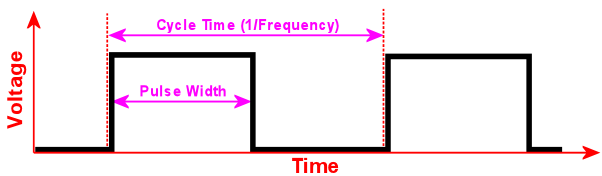
to any value from 8 Hz to 65535 Hz; the default setting is 20000 Hz.
The default setting was chosen to be high enough to be out of human hearing range, to minimize the acoustic noise that can occur when inductive devices like motors and solenoids are switched with PWM. Some such devices are vulnerable to mechanical vibration at PWM frequency, which manifests as acoustic noise. One way to address this is to raise the frequency until it's too high for human ears to detect. However, some amplifier devices can't switch above a limiting frequency, so the rate is adjustable in case you need to change it for compatibility with amplifiers or other circuitry on the outputs. Changes to the frequency setting are applied immediately. When changing the frequency, FREQL and FREQH should always be written as part of the same I2C transaction, to ensure that the device reads the new 16-bit value coherently. |
| 0x1B | FREQH | High byte of the 16-bit PWM frequency. |
| 0x1E | VERSION | Read-only: contains the current software version. This currently reads as 0x01. This will be updated if future versions change any aspect of the interface that a host might need to detect in order to take advantage of new features. |
| 0x1F | WHOAMI | Read-only: contains a signature value that identifies the device. This always reads as 0x24. WHOAMI registers are common in I2C devices, to provide the host with a simple sanity-check that the device it's addressing is the type of chip it expects and that the I2C connection is conveying data properly. |
| 0x20 | CONF0 |
OUT0 Configuration Register (CONF0). This register contains bit-mapped
flags controlling the configuration for the OUT0 output port:
|
| 0x21 | LIMIT0 | OUT0 Flipper Logic Power Limit Register. This sets a maximum power level for the port, on the same 0-255 scale used for the LEVELn registers. When the port's LEVEL0 register is set to a value greater than the LIMIT0 value, the device starts a timer on the port. When the timer reaches the time limit specified in the TIMELIMIT0L/TIMELIMIT0H registers, the device automatically reduces the port's actual output level to the LIMIT0 value. The limit remains in effect until the host makes a change to the LEVEL0 value that takes it below the limit. |
| 0x22 | TIMELIMIT0L |
OUT0 Flipper Logic Time Limit Register, low-order byte. Together with
TIMELIMIT0H, this sets a time limit, in milliseconds, that the port's
output level is allowed to exceed the LIMIT0 register value. After
the timeout expires, the port's physical duty cycle is reduced to the
value in LIMIT0. Once the timeout expires, the lower limit remains
in effect until the host sends a command to change LEVEL0 to a value
at or below the LIMIT0 value. This ensures that the port will be
held at the reduced power level in the event that the host software
crashes or otherwise malfunctions, leaving the port stuck at an
unsustainably high power level.
The TIMELIMITE0L and TIMELIMIT0H registers should always be written as a pair in the same I2C transaction, to ensure that the PWMWorker software reads the two bytes of the 16-bit value coherently. |
| 0x23 | TIMELIMIT0H | High-order byte of the 16-bit Time Limit Register for port OUT0 |
| 0x24 | CONF1 | OUT1 Configuration Register; same usage as CONF0, applies to output port OUT1 |
| 0x25 | LIMIT1 | OUT1 Flipper Logic Power Limit Register; same usage as LIMIT0, applies to port OUT1 |
| 0x26 | TIMELIMIT1L | OUT1 Flipper Logic Time Limit Register, low-order byte |
| 0x27 | TIMELIMIT1H | OUT1 Flipper Logic Time Limit Register, high-order byte |
| 0x28-0x7F | CONFn, LIMITn, TIMELIMITnL, TIMELIMITnH | Port register groups for OUT2 through OUT23, arranged in repeating 4-byte blocks, following the same pattern as the OUT0 registers |
| 0xDD | SWRESET |
Software Reset register. This register lets the host perform a
CPU reset on the PWMWorker Pico, which can be useful to ensure
that the device is in its initial power-on reset state. In
addition, the host can reset the Pico into its native Boot Loader
mode, which makes the Pico appear as a virtual USB thumb drive,
allowing the user to install new firmware over the USB connection.
To prevent accidental reboots due to errant or random writes to the register location, the SWRESET register only triggers a reset when a specific sequence of bytes is written, within a limited time. The host must first write the "start" byte, 0x11, then write the desired reset command byte within 5 seconds. The writes must necessarily occur in separate transactions, since each write within a transaction increments the destination register address automatically. The valid sequences are:
After completing one of these write sequences, the Pico will reset after a brief delay (around 50us). The delay is to help ensure that the reset doesn't interrupt the I2C transaction in progress, so that the host sees the normal end-of-transaction signals on the bus. The host should allow enough time for the device to complete the Pico hardware reset and PWMWorker's software initialization before addressing the device again; 10ms should be ample. When the device is reset into Boot Loader mode, it won't appear on the I2C bus again as long as it's in that mode, since the PWMWorker firmware won't be running. Returning from Boot Loader mode requires user intervention or a power cycle on the Pico. |
The LEVELn ports are all arranged in single contiguous block, from address 0x00 to 0x17. This is intended to allow the host to minimize I2C traffic by consolidating a level update affecting several output ports into a single I2C transaction. The typical usage pattern during normal operation is that the PC host will send the I/O controller updates via USB every few milliseconds, and the I/O controller will put these into physical effect on the PWM devices by sending I2C commands updating the device-side levels. These level updates are typically the only traffic during normal operation, so arranging the level registers in a single block helps minimize I2C traffic by allowing any contiguous block of levels to be updated in a single I2C write transaction, without the need to touch any registers other than the level registers.
The other per-port registers - CONFn, LIMITn, TIMELIMITnL, TIMELIMTnH - are arranged in groups by port. To calculate the address of the register group for OUTn, use 0x20 + 4*n. Then add 0 to get CONFn, 1 to get LIMITn, and 2 to get TIMELIMITnL. The rationale for grouping these registers by port is that all of these registers are for configuring the port rather than setting its output level. The host will often want to update all of the configuration registers for a given port together, so this grouping allows a single port's configuration registers to be updated in a single non-stop I2C write. The grouping makes it equally possible to update all of the configuration registers for all ports, or all of the registers for a contiguous block of ports, in a single write.
PWMWorker software for Raspberry Pi Pico, and accompanying documentation
Copyright 2024 Michael J Roberts
Released under a BSD 3-clause license
Redistribution and use in source and binary forms, with or without modification, are permitted provided that the following conditions are met:
1. Redistributions of source code must retain the above copyright notice, this list of conditions and the following disclaimer.
2. Redistributions in binary form must reproduce the above copyright notice, this list of conditions and the following disclaimer in the documentation and/or other materials provided with the distribution.
3. Neither the name of the copyright holder nor the names of its contributors may be used to endorse or promote products derived from this software without specific prior written permission.
THIS SOFTWARE IS PROVIDED BY THE COPYRIGHT HOLDERS AND CONTRIBUTORS “AS IS” AND ANY EXPRESS OR IMPLIED WARRANTIES, INCLUDING, BUT NOT LIMITED TO, THE IMPLIED WARRANTIES OF MERCHANTABILITY AND FITNESS FOR A PARTICULAR PURPOSE ARE DISCLAIMED. IN NO EVENT SHALL THE COPYRIGHT HOLDER OR CONTRIBUTORS BE LIABLE FOR ANY DIRECT, INDIRECT, INCIDENTAL, SPECIAL, EXEMPLARY, OR CONSEQUENTIAL DAMAGES (INCLUDING, BUT NOT LIMITED TO, PROCUREMENT OF SUBSTITUTE GOODS OR SERVICES; LOSS OF USE, DATA, OR PROFITS; OR BUSINESS INTERRUPTION) HOWEVER CAUSED AND ON ANY THEORY OF LIABILITY, WHETHER IN CONTRACT, STRICT LIABILITY, OR TORT (INCLUDING NEGLIGENCE OR OTHERWISE) ARISING IN ANY WAY OUT OF THE USE OF THIS SOFTWARE, EVEN IF ADVISED OF THE POSSIBILITY OF SUCH DAMAGE.