79. IC Chips
Integrated circuit (IC) chips are ubiquitous in modern electronics,
and you'll find several of them on the Pinscape boards. An IC is
essentially a miniature circuit board consisting of a collection of
the more basic components (resistors, capacitors, and transistors)
that we use elsewhere in our own circuit boards. There are ICs for
thousands of different functions and applications, ranging from simple
things like resistor arrays to complex computing tasks like running
Windows.
We'll start with some general information that's common to most IC
chips, then look at each of the specific chip types used in the
Pinscape boards. If you're working on building the boards
and you're trying to figure out how to install a particular chip, look
for the section on the chip in question later in the chapter.
Static electricity warning
Almost all IC chips are sensitive to static electricity. Refer to
Static Electricity Precautions for tips on handling static-sensitive parts.
Identifying a chip
Most chips can be identified pretty easily by the number printed
on the top of the case.
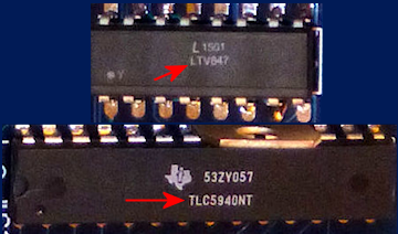
Each chip pictured above has two lines of random-looking alphanumeric
strings. This is pretty typical, but it's not any kind of standard;
some chips might have more or less printing, which might be arranged
in other formats. Whatever the format, the chip name should always be
in there somewhere. That should match the name that's used in the
schematic and printed on the board. Anything else is usually opaque
manufacturing codes not meant for our eyes, such as lot numbers and
date codes. How do you pick out the chip name from the other stuff?
You pretty much have to figure it from context, by looking for a chip
name you recognize. Somewhere in there, you should find the name of
the chip as shown in the schematic and on the PCB silkscreen.
Note that the name printed on the chip sometimes has slight variations
from the name used in the schematics. In particular, there might be
some extra prefix or suffix characters. These usually denote
variations of the chip, or different manufacturers, which have already
been accounted for in the parts list. Even so, if you do find such a
discrepancy, it might be worth double-checking the part list to make
sure you haven't accidentally swapped two parts that have similar names.
Chip orientation
Orienting a chip properly before installing it is critical. In the
best case, a chip that's installed in the wrong orientation simply
won't work, and in the worst case, the error might destroy the
backwards chip, or even other components, when you turn on the power.
So always make sure you have the right orientation before soldering
anything.
Most of the chips used in the Pinscape boards are "DIP" (dual in-line
package) chips with two rows of pins sticking out. It's easy to
tell which side is the top and which is the bottom: the pointy ends
of the pin point down, since they go through matching holes in the
circuit board.
What's not as obvious is the proper rotation. DIP chips are
rotationally symmetrical: they'll fit the space on the board if
you rotate them 180° from their proper orientation. So you
have to be careful to get that right.
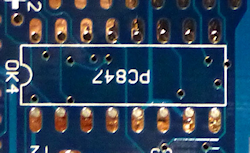
When you look at the Pinscape boards, you'll see little outlines for
all of the chips printed on the top of the board. Most of the IC chip
outlines look roughly like this:
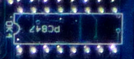
The first thing to note is the printing inside the outline, in this
case "PC847". That's the name of the chip to install here. When
you're about to plop a chip into position, it's always a good idea to
double-check that the name printed on the chip matches the name
printed on the board. Different chips can sometimes share the same
footprint, so it's good to make the extra check.
Don't be distracted by the fact that the writing is upside-down. The
text printed on the board is almost all oriented the same way with
respect to the overall board, for the readability's sake. If the text
were printed at all sorts of different angles across the board, it
could make some of the legends hard to read or even ambiguous (e.g.,
is that an "N6S" or an "S9N"?). The trade-off is that this often
makes the text appear upside-down or sideways with respect to the
component it refers to, as in this case. The important thing to
remember is to always pay attention to the outline, not the text, to
determine which way a component goes.
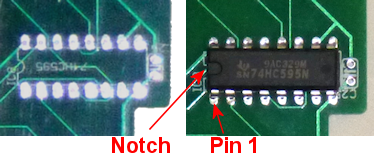
Which brings us to the second big feature in the photo: the notch.
That's the most important feature of the outline, because it's your
key to orienting the chip properly.
Whenever you see a notch in a chip outline like this, turn the board
so that the notch is at the left like in the photo. In that
orientation, pin 1 is the bottom left pin, just below the notch.
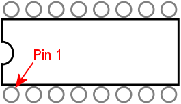
Now you know where pin 1 goes on the board, so all you have to do
is match that to pin 1 on the chip.
Some chips have the same type of half-circle notch that's printed on
the circuit boards. The notch in the chip isn't usually printed in
ink, though - it's usually a slight indentation or depression in the
plastic case. When you find a notch on the chip, orienting it to the
diagram on the board is easy: just line up the notch on the chip with
the notch printed on the board.
Not all chips use the notch, though. The other common convention
is a little circular "dot" in one corner. The dot is sometimes
marked in ink, and other times it's just a subtle indentation in
the chip casing. When there's a dot, it's in the corner nearest
to pin 1.
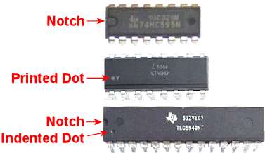
Common orientation markers on IC cases.
Some ICs have indented notches on one side; simply line this up
with the notch in the printed outline on the circuit board.
Other chips use a "dot" at one corner of the chip to mark the
location of pin 1. The dot might be printed in white ink, or
might be indented in the plastic.
If you don't see the notch or dot, it might just be a really subtle
one that's hard to spot. Look at the chip under a strong light,
and hold it at different angles. The indentation for the notch
or dot is sometimes very slight.
Once you find the notch or dot, it's just a matter of lining up
pin 1 on the chip with pin 1 on the board.
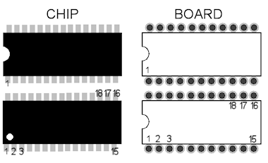
Examples of how to match the chip marking
with the board marking to find the proper orientation. Top:
the chip has a notch in its case like the one printed on the
board, so simply line up the notch on the chip with the one
on the board. Bottom: The chip has a dot near one corner.
Orient the chip so that the dot lines up under the notch
printed on the board.
Sockets
There are two main ways to install a DIP-type chip on the circuit
board: solder it directly to the board, or use a socket.
A socket is a receptacle that matches the exact footprint of an IC
chip. It has pins coming out the bottom, matching the pins on the
chip. You fit the socket's pins through the holes in the board
intended for the chip, and solder the socket pins to the board. The
top of the socket has matching openings for the chip's pins. Once the
socket is soldered to the board, you just plug the chip into the
socket. The pin openings in the socket are spring-loaded, so they
hold the chip in place without having to solder the chip.
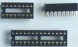
IC sockets: top view of a 16-pin socket;
side view of 16-pin socket; top view of 28-pin socket. Note
the notch at the left side in the top views: this has the same
purpose as the notch printed on the circuit board outline of
the chip, to serve as an orientation guide. Line up the
notch on the socket with the notch printed on the board
when installing the sockets.
The main advantage of using a socket is that it makes it practically
effortless to remove and replace a chip. That's a great time-saver if
you find that one of your chips is defective, or if it ever fails
later, or if you accidentally install it backwards on the first try.
In contrast, it's extremely difficult to remove a chip that's been
soldered directly to the board. It only takes a tiny bit of solder on
each pin to make it stick, and it's next to impossible to get all of
the solder off all of the pins on a large chip.
I recommend using sockets for all of the large chips, but it does
slightly increase the cost, so some people prefer to solder the chips
directly.
If you use sockets, note that each socket has a notch cut into the
plastic. This is meant to mimic the notch in the chip outline printed
on the circuit board, to serve as the orientation marker. You should
be sure to line up the notch in the socket with the notch printed on
the circuit board when you install each socket. That way, you can
use the notch in the socket as a proxy for the notch in the circuit
board chip outline when plugging in the chip - which is important
because the printed outline will probably be hidden behind the socket
once the socket is in place.
How to install a chip on a circuit board
If you're using a socket, follow the procedure we're about to describe
for soldering the chip, and just substitute the socket for the chip in
all of the steps. After the socket is installed, plug the chip into
the socket, taking care to orient the chip properly as described
above.
To solder a chip (or socket) to the board, first find the outline
printed on the board for the chip. Most IC chip outlines look
roughly like this:
Check that the chip type printed on the board matches the chip you're
getting ready to install.
Line up the chip's or socket's pins with the holes along the edges of
the outline. The number of holes should match the number of pins.
Carefully insert the pins through the holes.
Make sure the chip is oriented properly, as described above. This
is an excellent time for the "measure twice, cut once" rule - check
and double-check that you have the chip turned the right way.
Now insert the pins into the holes.
With DIP chips (the ones with two rows of pins), the pins are usually
angled out just a little wider than the holes, so you usually have to
bend one row of pins inward very slightly to fit them through the
holes. To make this easier, I like to start by inserting one row of
pins first. Then you can apply a little pressure to the whole chip to
uniformly bend the now-seated pins enough to fit the opposite row
through its holes. (Sockets don't usually require this kind of
maneuvering, since their pins stick straight down. It's another way
sockets make things a little easier.)
Inspect the pins from the top to make sure they all got seated
properly. It's easy for one or two pins to miss their holes and go
sideways when you seat the rest. If this happens, you
might be able to nudge the missing pins into their holes if they're
not too far askew, but don't force anything. The pins are delicate
and don't stand up to much bending and re-bending. If necessary, take
the chip back out, carefully (very carefully) straighten any pins that
went sideways, and try again.
Once you're satisfied that all of the pins made it into their
respective holes in the board, hold the pin in place from the top and
flip the board over. Verify that all of the pins really made it
through the openings, as seen from the bottom of the board.
If everything looks good, it's time to solder the pins in place.
Keep the board flipped over and solder the pins from the bottom.
Solder a pin at one corner first (any corner will do). You should
hold the chip firmly in place against the board from the other side
during this step to make sure that gravity isn't pulling it a little
away from the board.
Check again that the pins are still all in place. They
can sometimes work loose during all of this board flipping and
soldering.
If everything is still in place, solder the pin at the diagonally
opposite corner next, still holding the chip pressed firmly against
the board from the other side.
Do one more check that the pins are all still where they should be.
This is basically the point of no return - it's not too difficult to
get the chip free if necessary with only the two pins soldered, but
it'll be practically impossible once you solder more pins. So it's
worth making sure that everything is good before going on.
At this point, the two attached pins at the diagonal corners should be
enough to secure the chip mechanically, so you shouldn't have to worry
about anything coming loose from this point forward. You can just
work through the rest of the pins one at a time to solder each one in
place.
Pin numbering
All of the pins on a chip are numbered, for the purposes of
identifying them in the schematic.
The pin numbers are irrelevant when you're installing a chip, since
all you care about is getting the orientation right. However, you
might find a need to cross-reference the individual pin connections in
the schematic with the physical boards if you ever have a problem that
requires debugging with a voltmeter. If you ever have a problem with
the boards, one of the first debugging tasks will likely to be check
the continuity between various points on the board, to make sure that
pins that ought to be connected actually are connected.
Fortunately, pin numbering on the physical chips is pretty
straightforward, and better yet, it's highly consistent across
different kinds of chips.
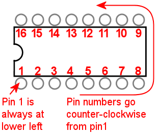
The Pinscape boards mostly use DIP chips - the type with two rows
of pins on opposing sides of the plastic case. All DIPs follow these
rules:
- Pin 1 is at the lower left (with the chip properly oriented)
- Pin numbers increase counter-clockwise around the chip
Chip symbols on schematics
The schematic symbols for chips can vary a little bit. There are a
few types of chips that have special symbols because of the function
they perform. Most chips, however, are so specialized that there's no
special symbol for them, so they're shown on schematics quite
generically, as simple rectangles with lines sticking out to represent
the pin connections. For example, here's the symbol for a TLC5940,
which is the large PWM controller chip used on the Pinscape expansion
boards for feedback device outputs:
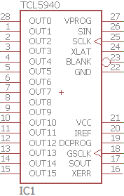
The rectangle represents the TLC5940 package, and the little lines
sticking out from the sides represent the pins. Note how every line
has a number. Those are the pin numbers, and they correspond to the
physical pin numbers we described above. You can use those numbers to
match up every pin on the schematic with the corresponding physical
pin on the board, which is important when you're trying to debug a
problem.
If you look closely, though, you'll see that the numbers shown on the
schematic aren't in the same order as the physical pins. That's in
keeping with the whole idea of a "schematic" - an abstract
representation that only keeps the essential information. Even so, it
might seem like it would be simpler if they'd use the same pin
ordering, but there's a reason they don't. To understand the
reasoning, look at the labels inside the TLC5940 box. Those are the
"names" of the pins, which are just arbitrary mnemonics that are there
to help a circuit designer remember the function of each pin without
having to memorize all the numbers or constantly refer to the data
sheet. Notice how the whole left side is OUT0, OUT1, OUT2, etc.
Those pins are all of the PWM outputs. On the physical chip, they're
not all together, but they're grouped on the schematic. That keeps
the schematic drawing a little neater.
In any case, the important thing to take away from this is that
you shouldn't pay any particular attention to the order of the pins
shown on the schematic; just pay attention to the numbers. Every
pin's number is explicitly shown, so you don't have to remember
a counter-clockwise or anything else; you just look at the numbers
printed there.
In the sections below on the specific chips making up the Pinscape
boards, we'll show each chip's exact symbol so that you can more
easily recognize it on the schematics.
Selecting chips
When you're ordering parts, the basic rule for IC chips is that you
should exactly match the chip name shown on the parts list.
This doesn't mean you have to get the exact Mouser part number listed.
That's different from the chip name; the Mouser part number is
Mouser's catalog ID, which encodes the manufacturer as well as the
chip type. Many chips are only made by a single manufacturer, so in
those cases they amount to the same thing. However, some chips are
generic, and interchangeable versions are made by several different
manufacturers. In these cases, the different manufacturers will all
use the same chip name, because that describes the specific function
and electrical characteristics of the chip, but the different version
will have different Mouser catalog numbers. So the thing to pay
attention to is the chip name.
If you find parts that have similar but not identical chip names, it's
better to err on the side of caution and assume they're different.
There are some very different chips with confusingly similar names out
there. If you think you found a match with a slightly different name,
the only way to be sure is to carefully compare the data sheets for
the two parts and make sure they really are functionally equivalent.
Chips on the Pinscape boards
555/7555 timer
The 555 is a venerable and widely-used timer chip. The Pinscape
boards use it (or more specifically, a variant called the 7555) to
implement the "timer-protected outputs" for the replay knocker and
chime outputs.
The 7555 is a more modern CMOS version of the original 555. The
Pinscape boards use the 7555 because it integrates better with logic
circuitry than the regular 555.
When buying parts, be sure to buy the 7555 when the parts list calls
for it, not the original 555 or other variant. The variants all come
in the same package and have the same pin layout, so they'll
physically fit the sockets, but there are some differences in their
electronic properties.
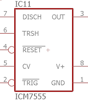
On a schematic, a 7555 is depicted with the generic IC box diagram,
with eight pins. "ICM7555" is printed near the box to identify the
chip type. The component name for a 7555 is of the form ICn.
The physical chip is an 8-pin DIP. My samples have an
easily visible notch for orientation. To install on the circuit
board, just line up the notch on the chip with the notch in
the chip outline printed on the circuit board.

7555: chip package, circuit board outline,
and chip installed in circuit board. Line up the notch on the
chip with the notch printed on the circuit board outline to
orient the chip properly. The writing on my sample chip is
so faint that you can barely see it in the left photo, and
can't see it at all in the right photo, but you can see it
on the actual chip with the right lighting.
LD1117AV33 3.3V regulator
The Pinscape boards use a type of chip known as a voltage regulator to
supply 3.3V to some of the logic chips on the boards. The part name
for the 3.3V regulator we use is LD1117AV33. Similar regulators are
available for numerous other voltages, but the Pinscape boards currently
only use the one type.
When buying parts, don't try to "fuzzy match" the name of this chip
with similar-looking parts, because suffix in this case ("AV33") is
highly significant: it indicates the regulated voltage. That's a
critical element of the circuit design. Similarly named chips with
slightly different suffixes regulate to different voltages, so they
won't work as substitutes.
These chips don't come in the usual DIP form factor. Instead, they
use a type of package more commonly used for transistors, known as
a TO-220. Here's what it looks like:
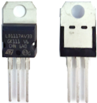
Front and back view of LD1117. Note that the part
name is printed on the front of the plastic case to help identify
the part.
Note that the TO-220 package type is widely used for other, completely
different components, particular MOSFETs and power transistors.
Anything in a TO-220 looks just like this, so you can't identify an
LD1117 by the shape of the case alone. For positive ID, check the
markings on the case. For this part, the chip name (LD1117AV33) should
be printed on the front of the plastic case.
On the schematic, these chips are shown with the standard generic IC
box diagram, with three pins. However, unlike most IC box symbols,
these don't show any pin numbers. They only show mnemonic labels for
the pins. The reason is that there aren't any standard pin numbering
conventions for the TO-220 package used for this chip, so pin numbers
would only be confusing. This is a case where you have to look at the
data sheet to figure out the correspondence between the pins on the
schematic and the physical pins on the device. But we'll save you the
trouble:

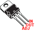
Above left: the LD1117 voltage
regulator symbol on a schematic. Above right: diagram of the
package showing how the physical pins relate to the pins on
the schematic symbol. The package diagram shows the
"front" of the package, with the black plastic case facing the
viewer. The back of the chip is the big metal fin, visible in
the diagram sticking out from the top.
The component ID shown on the schematic for these chips uses
the typical form for IC chips, ICn.
On the circuit board, the LD1117 doesn't use the standard
notched-rectangle outline, in keeping with its unusual packaging.
Instead, it shows an outline with a heavy bar on one side, which
represents the big metal fin on the back of the chip package:
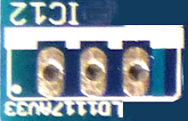
To install the chip in the circuit board, orient it so that the
metal fin on the back of the chip lines up with the heavy bar
printed on the PCB outline. The heavy bar in the outline represents
the fin, so you just need to make sure the actual fin is oriented
on the side indicated on the outline.
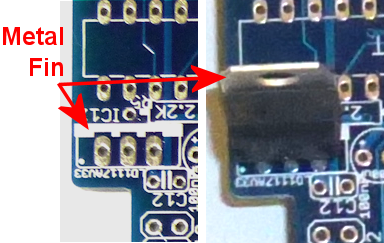
When you install the chip in the board, note that the plastic package
won't quite sit flush against the board. The legs have kinks near the
tops (the case side) that act as stops, which will keep the plastic
case part a couple of millimeters above the board surface. That's
perfectly normal; don't try to force the kinks through the holes. The
extra distance from the board is there by design, to help the fin
radiate heat more efficiently. You can be sure that any part you see
with a big metal fin like this is something that gets hot in normal
use, and the fin is there as a heat sink.
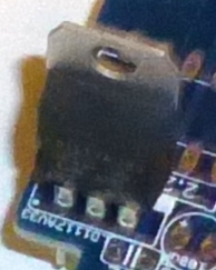
To install this chip, insert it through the holes, checking that the
fin is oriented to match the heavy bar in the outline printed on the
board. Flip the board over (taking care to hold the chip in place so
that it doesn't fall out), and solder the three pins to the pads from
the bottom of the board. The leads on these chips are quite long and
will stick out about a centimeter from the back of the board when
you're done, so you should trim the excess with wire cutters after the
chip is in place. Trim the leads to be roughly flush with the top of
the solder ball.
ULN2064B Darlington transistor array
The ULN2064B is an array of four Darlington transistors. Darlingtons
are high-gain transistors that can be used for amplifiers, or in our
case, switching medium-power loads from logic circuits. These chips
can handle loads up to 1.5A on each output. The Pinscape main boards
use these for the flasher LED outputs, because they have plenty of
power capacity for large LEDs and are physically compact.
This chip uses the standard generic IC box symbol on schematics,
with 16 numbered pins. The component name shown on the schematic
uses the form ICn.
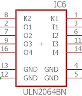
The physical chip is a standard 16-pin DIP.
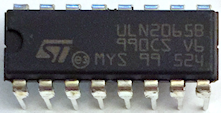
ULN2065B 16-pin DIP package. The half-circle
notch (visible at the left edge of the package) serves as the
orientation marker when installing. Line up the notch on the chip
with the notch in the chip outline printed on the board. Note that
this is the ULN2065B, which can be substituted for ULN2064B.
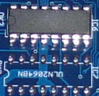
On the circuit board, the location for this chip is shown with the
usual chip outline, with "ULN2064BN" printed in the outline. Line
up the notch on the chip with the notch in the printed outline
to orient the chip properly.
Substitutions: The ULN2065B can be substituted for the
ULN2064B. The two are almost identical chips, the only difference
being that the 2065 is rated for higher maximum voltage. In other
words, the 2065 is just a slightly tougher version of the same chip.
PC817 optocoupler
The PC817 is an optocoupler, which is a device that connects two
circuits via light signals rather than electronic signals. The light
signals are transmitted by a tiny IR LED inside the chip, and are
received by an adjacent phototransistor. (All of the light
transmission happens inside the chip, so you won't see light coming
out of it, and you don't have to worry about interference from ambient
light. An optocoupler isn't the same as an "opto interruptor", which
is a kind of switch that's controlled by blocking and unblocking a
light beam, like an electric eye. An optocoupler doesn't have an
exposed beam that you can block.)
This might sound like a lot of trouble - turning electrons into
photons, and then turning the photons back into electronics. But it
serves a very useful purpose: it lets the two circuits transfer
signals without any electrical contact. That has many applications,
but the one we use it for in the Pinscape boards is to create a sort
of safety barrier between logic circuits and power circuits, to help
protect the logic circuits from the higher voltages and currents used
in the power circuits.
On a schematic, the PC817 looks a little different from other ICs,
because it doesn't use quite the same generic IC box. Optocouplers
are important enough in electrical engineering practice that they have
their own special symbol:

If you ignore the interior of the box, you'll see that this actually
does still follow the same pattern as the generic IC box: it's still a
box with lines attached representing the IC pins, and the pins are
numbered as usual. What's different is that the interior of the box
shows symbols instead of mnemonic labels for the pins. To an engineer
who knows the language, the symbols are the equivalent to the mnemonics
used on other chips, in that they indicate the functions of the pins.
The symbol on the left side of the box represents the phototransistor
that receives the optical signal; the symbol on the right represents
the LED that transmits the signal; and the two diagonal arrows in the
middle represent the photons carrying the signal from the one side
to the other.
You might also notice that this chip's component ID is "OKn"
instead of the usual "ICn". This is an EAGLE-ism; "OK"
probably stands for "Opto-Koupler", and I'm not sure why they chose
"OK" rather than "OC", but at a guess it's to avoid confusion with "C"
for "capacitor". At any rate, just be aware that the schematics and
parts lists use this unusual "OKn" designation for these chips,
even though they're like any other ICs for all practical purposes.
The physical chip is a 4-pin DIP:
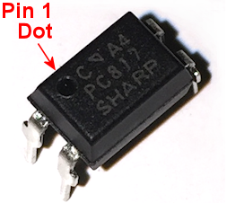
The orientation marker on these chips is usually the "pin 1" dot,
in the corner nearest pin #1. The chip in the photo above uses the
indentation form of the dot, but yours might have a printed white
dot instead. As always, the dot can be such a subtle indentation or
faint ink mark that it's tough to see without a strong
light and/or magnifying glass.
This chip's proportions are unusual for a DIP, which can be confusing.
You get accustomed to all the other DIP chips being wider than they are
tall. So it can be tempting to think that this one needs to be
rotated into "landscape mode", with the pins at the left and right
sides. That's even the way the printing on the chip is aligned,
because of the limited space. But consistency is the key here: this
is still a DIP, so apply the standard DIP rules. When properly
oriented, the pins go along the top and bottom edges, and the pin 1
dot goes at the lower left corner.
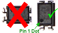
Orienting the PC817. Even though its "aspect
ratio" is unusual for a DIP, use the same orientation rules you'd use
for any other DIP chip, placing the pins along the top and bottom
edges and the "pin 1" dot at lower left.
On the circuit board, the slot for a PC817 is marked with the standard
IC outline, with the notch on the left side and "PC817" printed inside
the outline to indicate which part to install.

Install the chip like any other DIP. Hold the board so that the
notch in the printed outline is at the left side, and orient the
chip with the pin 1 dot at lower left.
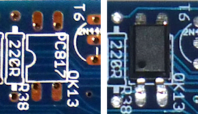
Substitutions: The LTV817 is equivalent to PC817.
PC847 quad optocoupler
The PC847 is a chip that consists of four PC817 units packaged into a
single IC. There's really no difference at all electrically or
functionally between one PC847 and four PC817 chips, but the quad
package is a little more convenient to work with when multiple
optocouplers are grouped in the same area of the board, simply because
it reduces the the number of parts you have to solder.
On a schematic, a PC847 is even represented just like it's four
separate PC817 chips. Which it really is, functionally speaking, and
schematics are all about function.

The schematic symbol for a PC847 chip consists
of four separate PC817 symbols. The only clue that they're the same
physical chip is the component ID: look for the A-B-C-D suffix, which
tells you the sub-unit within the chip.
There are a couple of things to notice. The first is that the
individual units all have the same "OKn" component ID, but each
one also has a suffix - A, B, C, D. The suffix tells you which
sub-unit we're talking about. The common OKn prefix is how we
know that these units are all part of the same physical PC847 chip.
In my own schematics, I also make a point of grouping the sub-units
together on the page, so that you don't have to go hunting around to
find all of them, but you might encounter cases in other people's
schematics where the sub-units aren't grouped.
The second thing to notice is the pin numbering. Note how the pin
numbers aren't grouped contiguously on each sub-unit. For example,
unit A uses pins 1, 2, 15, and 16. If you scan over all four
sub-units, you'll see that all 16 pins are accounted for (and each
appears exactly once).
The chip is packaged as a standard 16-pin DIP:

LTV847 (equivalent of PC847). These chips
use a (faintly) printed dot to mark the location of pin 1.
On the circuit board, a PC847 is marked with the standard IC
chip notched outline, with "PC847" printed inside to identify
the part to install there.

Installing a PC847 is just like any other DIP. Orient the board
so that the notch in the printed outline of the chip is at the
left side, then orient the chip with the pin 1 dot at the lower
left corner.
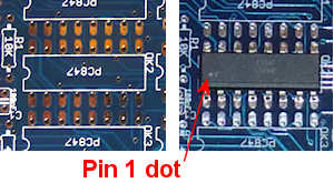
Substitutions: The LTV847 is equivalent to PC847.
TLC5940NT PWM controller
The TLC5940NT is a PWM (pulse-width modulation) controller chip. This
means that it generates a series of very fast and precisely timed
on/off pulses, under the control of a computer or microcontroller.
PWM has many uses, but for our purposes, it's a way to control the
brightness of a lighting device, the speed of a motor, or the force of
a solenoid. The Pinscape expansion boards use these chips to
implement the output ports on the main board and the power board.
The TLC5940 is a proprietary chip from Texas Instruments, and TI no
longer manufactures the DIP version used on the Pinscape boards. They
do still manufacture the same chip in "surface mount" packages, but
those aren't nearly as hobbyist-friendly as DIPs, so the Pinscape
boards still use the DIP version for ease of assembly. Fortunately,
the DIP version has always been extremely popular with robotics and
Arduino hobbyists, and perhaps as a result the supply continues to be
plentiful. That continues to surprise me, since TI hasn't made the
DIP version since about 2014, but some people conjecture that the
continuing supply is coming from gray-market versions manufactured by
(presumably unauthorized) third-party factories. Whatever the reason
for this good luck, the Pinscape boards will continue to use the DIP
version as long as it remains easy to find. If that ever changes,
I'll update the boards designs to use one of TI's newer PWM chips
instead. That will make assembly a little trickier, because those are
all surface-mount parts, but on the plus side, TI's newer PWM chips
have much nicer designs than the rather aged TLC5940.
On a schematic, the TLC5940NT appears as the standard generic IC
box, with 28 numbered pins.

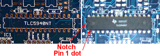
The physical chip is a 28-pin DIP.

Note that the sample pictured above has both the half-circle notch at
the left side and a "pin 1" dot, both as slight indentations in the
plastic. You might also notice larger, shallower circular depressions
centered vertically at either end of the chip. Ignore these; I think
those are just artifacts from the molding process that carry no
meaning. Just pay attention to the standard notch and dot markers.
On the circuit board, the TLC5940NT is marked with the standard
notched outline for an IC, with "TLC5940NT" printed within. To
install the chip, orient the board so that the notch in the printed
outline is at the left side, and then orient the chip so that pin 1 is
at lower left.
74HC595 shift register
A shift register is a logic chip that lets a microcontroller set the
on/off voltage states for a number of pins on the chip. The Pinscape
chime boards use these chips to control the outputs on the chime
board.
On a schematic, the 74HC595 is drawn with the usual IC box:
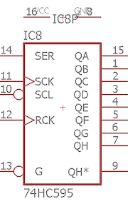
There is one unusual feature of this symbol that you might not even
notice if you saw it as part of a larger schematic, but it stands out
when we isolate the symbol like this. The unusual part is that
separate-looking bit at top. Above the chip box, the symbol shows two
of the IC's pins that aren't included in the box. The way you
can tell that those disembodied pins are part of the same chip is the
"IC8P" marking. The "P" suffix tells you that these pins constitute a
part of "IC8"; the "P" is for "power", as these are the power and
ground connections for the chip.
This use of separated schematic elements is somewhat reminiscent of
the PC847 that we saw earlier, where the individual optocoupler units
within the chip are drawn as separate boxes. In this case, the pins
are separated simply to reduce clutter within the box. The symbol's
designer thought that there were enough pins already and wanted to get
a few out of the way. The power and ground pins were elected because
they're givens in any chip. Some engineers just short-hand them away
entirely, leaving them off the schematics and letting the reader
assume they're connected in the standard way. I prefer showing them
explicitly, which in this case that means adding this little islands
of pins separated from the chip. I consider this style rather
obfuscatory, and fortunately this is the only chip in the Pinscape
boards that uses it.
The physical chip is a 16-pin DIP.

My samples have an indented notch on one side of the case to indicate
pin 1: as always, if you orient the chip so that the notch is at the
left side, pin 1 is the bottom left pin.. As always, this can vary by
lot, so yours might have a painted or indented "pin 1 dot" instead.
On the circuit board, this chip uses the standard IC notched outline,
with the part name (74HC595) printed within to identify the component
to be installed there. To install, orient the board so that the
notch in the printed outline is to the left, then orient the chip so that
pin 1 is at the lower left.
